Electron beam lithography is a system when concentrated electron beams are scanned to draw a specified form on a surface covered with an electron-sensitive film called a resistance. (Often shortened as electron lithography) (exposing). The electron beam alters resistance solubility, allowing either the exposed or the non-exposed resistant areas to be removed selectively by immersing it in a solvent (developing). Like photolithography, the aim is to generate extremely tiny structures in the resistor which may then, frequently by etching, be transferred to the substrate.
A focused power of the electron is scanned across a substratum coated with electron-sensitive material (resistance) which changes its solubility characteristics according to the energy deposited in the electron’s beam. The operating concept of EBL is quite simple and very comparable to photolithography.
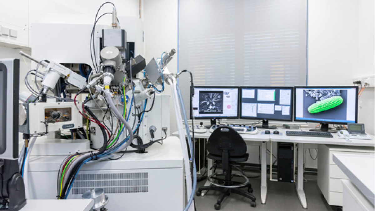
During EBL the electron beam concentrates on the substrate by use of an electron pistol contained within a very high column of vacuum. The electron beam is utilized to write photo-layer patterns. Because the exposure source is now practically an electron beam rather than UV. The main benefits of EBL are that patterns with a resolution of less than 10 nm may be entered.
The instruments are exceedingly unusual because of the very high electron beam lithography cost of capital (millions of dollars). Since EBL is an inherently extremely sluggish writing style. For this reason, EBL is usually exclusively utilized for mask design and advanced research and development applications. But what are the costs and runs for fixing electron beam lithography?
A pattern of transmission of electron lithography: The lithograph is generally the transfer by selective exposure to a radiation source as the light of a pattern in the photo-sensitive material. A photosensitive material is a substance that is subject to a radiation source that changes its physical characteristics. If a photosensitive material is selectively exposed to radiation (i.e. by masking some radiation), the radiation pattern on the material is transmitted to the exposed material, since the characteristics of exposed and exposed areas differ.
This debate, which focuses on optical lithography, is essentially electron lithography in the visible spectrum utilizing a radiation source with certain wavelengths. The photosensitive substance employed is usually a photoresist in the lithograph for micromachining (also called resist, other photosensitive polymers are also used). When a certain wavelength’s resistance is subjected to a radiation source, the resistance to the developer solution alters its chemical resistance. If after selective exposure to the light source, the resistor is put in a development solution, it removes one of the two areas (exposed or unexposed). The material is regarded as a positive resistance if it is grafted by the developer and the unexposed region is durable. If the exposed material is highly robust and if the exposed area is removed, the negative resistance is assessed.
Micromachining lithography is the main process for defining patterns. However, as the process is able to produce fine features economically, a photosensitive layer is typically employed as a temporary mask while grabbing a subordinate layer to transfer the pattern to the overlying layer. The photoresist can also be utilized as a patterning template for the lithography material. The resistor is then removed and the substance placed on the resistor ‘removes.’
For transferring a pattern from a resist to another layer, the deposition template (lift-off) method is less frequent than utilizing a resistance pattern as an etch mask. The reason is that resistance is not compatible with the majority of MEMS deposition methods, mostly because it does not resist high temperatures and can function as a source of contamination.
Usually, the resistor is removed after the pattern is transferred to another layer. This is typically essential because the resistance is incompatible with future processing stages. This is necessary. It also dramatizes the topography, which may impede future processes in lithography.
Alignment: The patterns for multiple lithographic processes belonging to one structure must be aligned to each other to create usable devices. The first model transferred on a wafer generally contains a set of alignment markers, which are very accurate features that relate to the first pattern when placed after the patterns. The initial alignment markings may be eliminated as the processing continues. Often aligner marks are incorporated in other patterns.
The mask function used to register the mask can be transferred to the wafer depending on the electron lithography system equipment utilized. In this scenario, the alignment marks may be identified in such a way that wafer processing or device performance is not affected thereafter. The transfer of patterns from the mask’s features to the wafer may erase the wafer’s alignment functions. The alignment markings should be constructed to minimize this impact or several copies of the alignment marks on the wafer should alternatively be available so that there are still alignment marks for additional masks to be registered.
Alignment notes may not necessarily be positioned on the wafer arbitrarily as the equipment used for alignment can only have limited movement and can only align itself with characteristics within a given region of the semiconductor. The shape and size of the region may also change with the alignment type so that before average marks are located, the lithographing equipment and alignment type must be considered. Usually, the alignment of the mask and the wafer is done in 2 marks, and the mask and wafer are aligned by one alignment mark to x and y but two marks are needed for the correction of the thin offset during rotation (ideally spaced away).
Since the wafer has no design to align with the first pattern, the first pattern is usually aligned with the main wafer. This can be done automatically or manually, depending on the lithographic equipment utilized or an explicit registration function for the wafer on the mask.
Exposure: For an exact pattern transfer from the mask to the photosensitive layer, the exposure parameters needed largely depend on the radiation source wavelength and on the dosage necessary to produce the desired photoresist change. Various photographers show various sensitivity for different wavelengths. The dosage necessary for successful pattern transfer per unit volume of photoresist is fairly constant; however, the physics of the process of exposure can change the dose actually received. An extremely reflecting layer under the photoresist, for instance, might result, when the photoresist is exposed to both radiations and reflected radiation, in the material that receives a greater dosage than if its underlying layer is absorbing. The dosage also varies with the thickness of the resistance.
Higher-order effects are also present, such as patterns of interference in thick resistant films, which can alter pattern quality and sidewall characteristics.
The dosage received by the photographers near the edge of the pattern light will become substantial if the photograph is over-exposed. By employing positive photo-resistants the photo-resistant picture will be degraded along the edge and the characteristic dimension will be reduced and sharpness or corners will be lost. If we have a negative resistor, then the photographic photo is dilated so that the features are larger than intended and the sharpness of the corners is lost again. If a picture is significantly underexposed, the pattern cannot be copied, and the results for over-exposure will be similar, in less severe situations, with the outcomes inverted in relation to various resistance polarities.
If the surface exposed is not flat, a loss of focus in the picture across the different topography might distort the high-resolution image of the mask on the Wafer. This is one of the limiting issues when high aspect ratios are present for MEMS lithography. Also, there are issues with achieving uniform resistant thickness coating, which further impairs the transfer of pattern and makes processing complicated.
The Lithography Module: Typically, a properly characterized module lithography involves wafer surface preparation, photographic deposition, mask and wafer alignment, exposure, development, and suitable resistance conditioning. To guarantee that the rest of the resistor at the end of the module is an optimum image of the mask and the appropriate sidewall profile, the lithographic processes must be defined as a sequence.
The standard steps found to fix EBL in a lithography module are: Dehydration bake, HMDS prime, resist spin/spray, soft bake, alignment, exposure, post-exposure bake, develop hard bake, and descum. Not all lithography modules will contain all the process steps and therefore fixing electron beam lithography won’t take 50 steps.