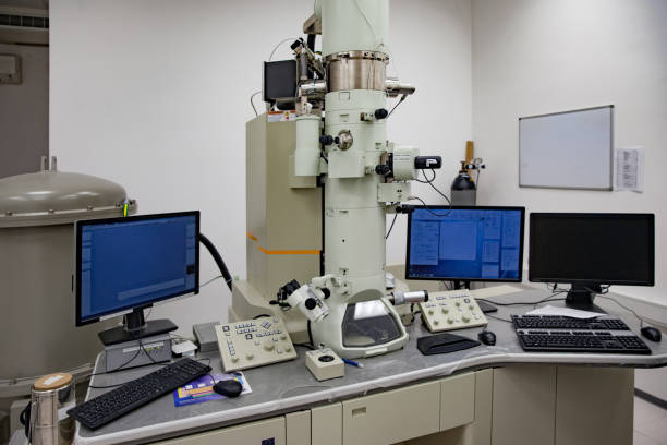
An electronic beam focused on a surface creates images under a scanning electron microscope (SEM). As electrons in the beam interact with a sample, they produce several signals that help determine the surface’s topography and composition.
Table of Contents
A light microscope as opposed to an electron microscope, what are the differences?
Human eyes can distinguish between two points separated by 0.2 mm inadequate light without any aid from additional lenses. A person’s resolving power is how sharply they can see detail. A lens or a group of lenses (e.g., a microscope) can provide viewpoints closer together than 0.2 mm.
Today’s light microscopes magnify images at a maximum power of about 1000x. An optical microscope resolving power can only be determined by the wavelength of light, the number of lenses, and the quality of illumination. From 400 to 700 nanometers (nm) are the wavelengths of white light. Light microscopes in white light have a theoretical resolution limitation (no visibility) of about 200 – 250 nm, as the wavelength averages out at 550 nm. A light microscope’s wavelength became its limiting factor, hence the development of the electron microscope. Because electrons are shorter in wavelength, they can provide a better level of resolution.
Scanning and transmission electron microscopy relies on focusing high-energy electrons (0.1-50 keV) onto the surface of a sample. There are several possible interactions, such as secondary electron emission, backscattered electron emission, photon emission, X-ray emission under certain conditions; excitation of phonons; and diffraction.
In all basic SEM systems, the detector records data about the surface under observation in the form of secondary electrons, which can have resolutions of 1-2 nm and magnifications from 10x to 500,000x. With appropriate detectors, you can collect data on compositions, phases, electrical properties, optical properties, and temperature properties. Material scientists probably consider the essential environmental scanning electron microscope to be the most versatile instrument. Additionally, it serves as a platform as well as an instrument. By combining the electron microscope with scanning probe microscopy (SPM), it is possible to enhance control over the manipulation of nanostructures or to specify a region of interest for observation with high precision. Measurements can be made for both processes since the bombarding electron beam can scan in the X-Y plane. The temperature can be gradually raised or lowered in a chamber to exhibit in situ phase transitions. When specimens are ready for transmission electron microscopy, the ion beam interacts with the laser. It is the scanning electron microscope principle.
In Semtech’s systems, there is a JEOL 6320F for the highest resolution imaging — which comes from a combination of its cold-field emission source, spectroscopy electronics, and in-lens detectors. The other equipment includes a Hitachi S-3400N variable-pressure reactor and JEOL JSM-5800, equipped with a spectral imaging system and scanning probe microscopy. When the quantitative composition of specimens is needed, the JEOL 8900L electron microscope is the preferred option.
SEM’s primary characteristics
- A high-speed acquisition (30-60 s) with high-resolution imaging (1-2 nm)
- An observation of the sample at 5-6 orders of magnification (10x to 500,000x)
- A non-destructive method
- It must be vacuum compatible. A vacuum chamber can accommodate specimens as large as four inches. Dimensions: diameter
- The multi-mode operation provides versatility.
- Easily accessible sections can be measured cross-sectionally.
A Scanning Electron Microscope Technique
- Scanning Electron Microscope resolution and Operating Modes
- Induced-Current-by-Electron Beams
- A cathodoluminescence reaction
- Atomic Diffraction by Backscattered Electrons
- Microscopy Platform with Scanning Probes
Electron transmission microscopy, transmission/scanning
An electron beam of single energy tends to bombard thin samples, typically less than 200 nm in thickness, in transmission electron microscopy (TEM). Electrons transmitted through the model can increase in strength by electromagnetic lenses that magnify the signal of the scattered electrons. Electron diffraction may produce colored signals, amplitude, phase-contrast imaging, diffraction contrast, high-resolution TEM, or amplitude-contrast imaging.

Programs and applications
- The Crystallographic Method
- Through electron diffraction, particles are examined on a fine-scale to determine their crystallographic structure.
The microstructure
In addition to providing information about the composition of materials, high-resolution TEM can give information about defects’ microstructure and atomic architecture. An atomic-resolution STEM Z-contrast imaging technique can deliver results that you can interpret directly, giving you atomic-resolution images of materials, blemishes, and interfaces in samples.
The composition
The EDS and EELS are capable of both quantitative and qualitative analysis of any element. With STEM EDS and EELS, one can map features down to a molecular scale. In addition to providing information on materials’ electronic properties, EELS also researches their structure. Through GIF, high-resolution element mapping can be available by energy-filtered TEM.
- An analysis of cross-sections
- Study of the structure, composition, degree of perfection, and properties of multilayered films and interfaces.
- An overview of Transmission/Scanning Transmission Electron Microscopy appears in the table below.
Aesthetics and medical science
SEMs are finding use in a variety of medical fields due to advances in medical science. Comparing blood and tissue samples is done using scanning electron microscopes. Medical professionals can use it to find the cause of a disease. The following are the areas of operations for these companies:
- Finding the causes of illness and the viruses that cause it
- New vaccines are in development
- Medications undergo testing
An SEM helps in testing samples to determine whether a patient is going to live a long time.
Therefore, the above experts can check how much is an electron microscope costs and use scanning electron microscopes for various development purposes.
Companies that specialize in search engine marketing may offer their services. The company can tell you more about the product’s applications and uses if you contact them. Ensure that the company has a good reputation and extensive experience before you hire them.

